Advanced Packaging Thermal Management Calculator
Input Your Design Parameters
Calculate heat dissipation requirements for your advanced packaging configuration
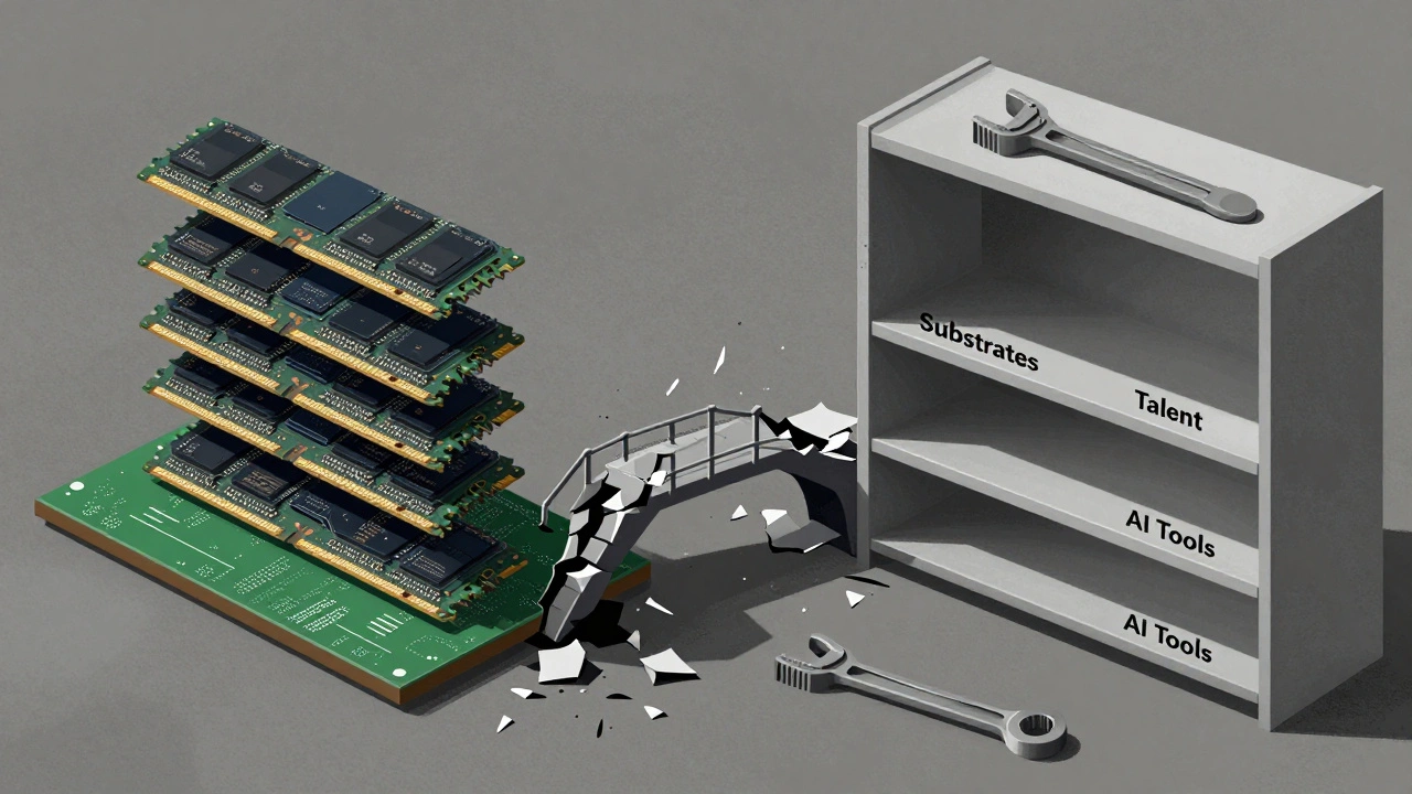
When you think of AI chips, supercomputers, or the latest smartphone processor, you probably imagine tiny transistors and complex circuitry. But what keeps those chips alive? It’s not just the silicon-it’s the advanced packaging holding everything together. In 2026, this hidden layer of semiconductor manufacturing has become the biggest bottleneck in tech innovation. We’re not talking about slow delivery times or stock shortages. We’re talking about real, physical, and human limits that are slowing down the entire industry. Three things are holding us back: substrates, tools, and talent. And right now, none of them are keeping up.
Substrates: The Foundation That Can’t Keep Up
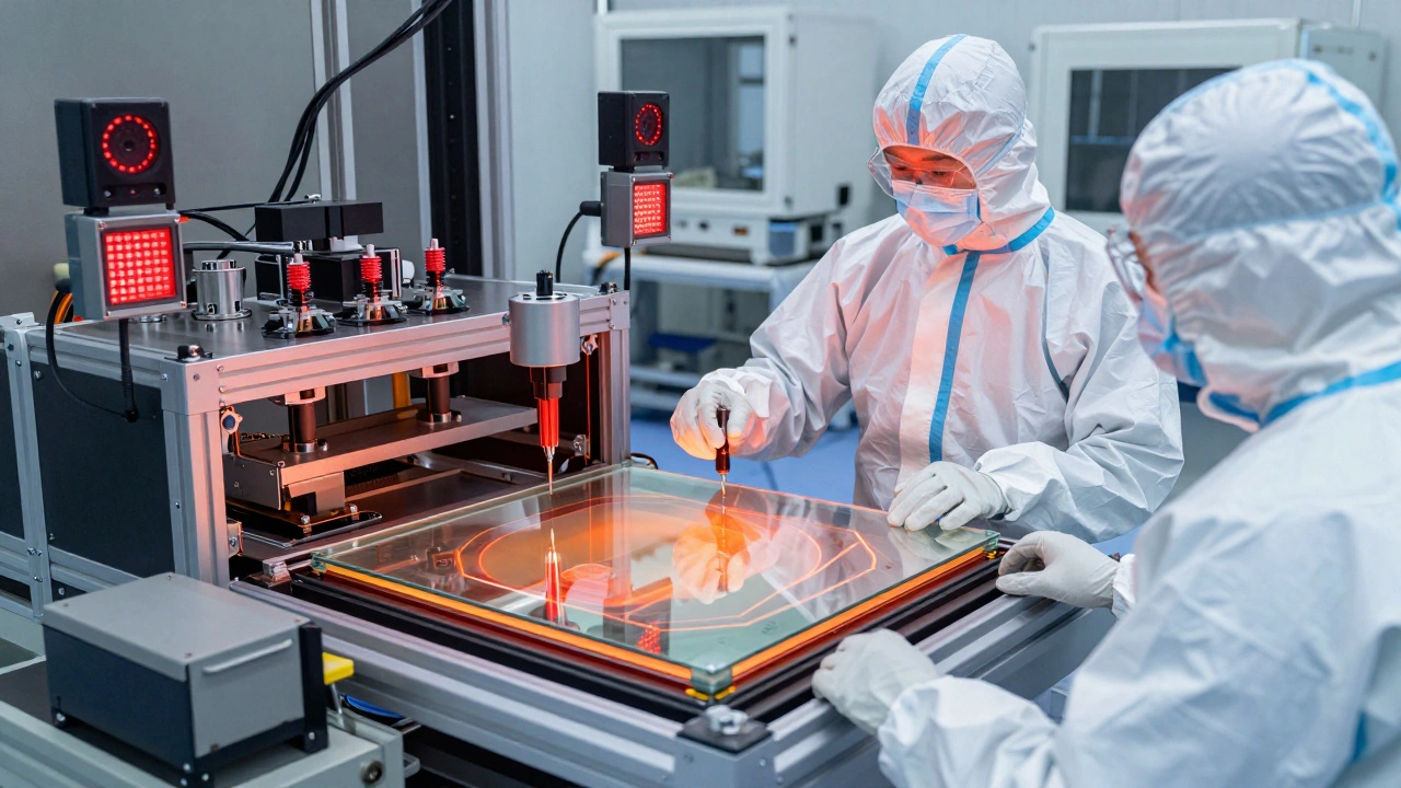
Think of a substrate as the foundation of a house. In advanced packaging, it’s the layer that connects chiplets, memory stacks, and optical interconnects. The industry is moving fast-from traditional wafer-scale packaging to larger panel and glass substrates. Why? Because AI chips need more connections, more power, and more heat dissipation than ever before. HBM stacking, chiplet integration, and Co-Packaged Optics (CPO) all demand substrates with higher density, better thermal performance, and tighter tolerances.
But scaling these new materials is hard. Glass and panel substrates require completely new manufacturing lines. Companies like TSMC and ASE are racing to build them, but each new facility takes years and billions to set up. Meanwhile, legacy wafer-based production still runs in parallel, splitting resources and slowing innovation. There’s a chicken-and-egg problem: you can’t design wafer-scale systems without AI-driven design tools, but those tools don’t exist because the packaging technology isn’t mature enough yet.
And it’s not just about size. Thermal management is a physics problem. When you stack 12 layers of chips and pack them with 10,000+ interconnects per square millimeter, heat doesn’t just go away. It builds up. No substrate on the market today can reliably handle the thermal load of next-gen AI processors without expensive liquid cooling or radical redesigns. This isn’t a software bug. It’s a law-of-physics limit-and we’re hitting it hard.
Tools: The Machines That Don’t Exist Yet
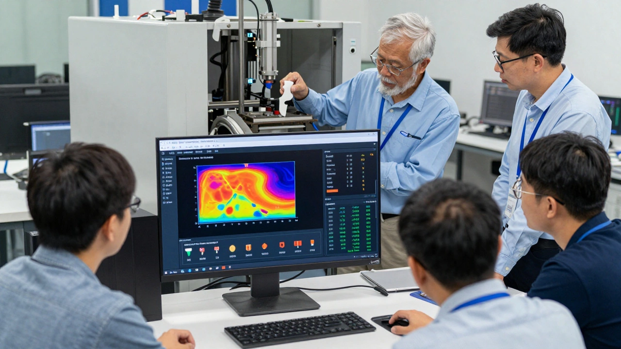
Advanced packaging isn’t just about materials. It’s about the machines that build it. The tools needed today-3D printing for spare parts, AI-driven inspection systems, automated optical alignment rigs-are not the same tools used ten years ago. And many companies are still using outdated equipment that can’t handle the precision required.
3D printing is one of the few bright spots. It’s no longer just for prototypes. In 2026, leading OSATs are using 3D-printed components to replace broken parts in packaging machines. Instead of waiting six weeks for a replacement part from Asia, they print it onsite in 48 hours. This reduces downtime by 60% and cuts inventory costs by nearly half. But here’s the catch: only 1 in 4 companies have the capital or expertise to deploy this. The rest are stuck with broken machines and long lead times.
Then there’s AI integration. According to the PROLOGIS 2026 Supply Chain Outlook, 70% of executives say they’re using AI to optimize their supply chains. That sounds good-until you realize that means 30% aren’t. Those companies still rely on spreadsheets, manual forecasts, and gut feelings. Without real-time dashboards tracking substrate inventory, tool utilization, or yield rates, they can’t predict shortages. They can’t reroute shipments. They can’t adjust production schedules. And when a single bottleneck in substrate supply delays a whole batch of HBM chips, the ripple effect hits everything from data centers to smartphones.
And let’s not forget the digital divide. Many packaging lines still have operators manually entering data into legacy systems. That’s not just slow-it’s error-prone. One miskeyed lot number can mean a $2 million batch gets scrapped. The industry needs integrated, cloud-based platforms that connect design, fabrication, and testing in real time. But building those systems? That’s a multi-year project most companies aren’t ready to fund.
Talent: The People Who Aren’t There
Here’s the truth no one wants to say out loud: we don’t have enough people who know how to do this work. Advanced packaging isn’t like assembling smartphones. It’s a blend of electrical engineering, materials science, thermal physics, and AI-driven manufacturing-all in one job. And there aren’t enough graduates with that skill set.
Universities are still teaching traditional semiconductor processes. But today’s packaging engineers need to understand heterogeneous integration, optical interconnects, and how to optimize thermal paths across 3D stacks. They need to know how to work with AI tools that predict yield loss before a wafer even gets processed. They need to collaborate with fabless designers who don’t speak the same language as assembly teams.
The talent gap is real. In the U.S., fewer than 500 engineers graduate each year with specialized training in advanced packaging. In Europe, it’s worse. China is training more, but their workforce is stretched thin. Meanwhile, wages are rising. A senior packaging engineer in Taiwan now earns 40% more than they did in 2020. And even then, companies can’t find enough qualified applicants.
It’s not just engineers. Technicians who run the machines? They’re aging out. Fewer young workers are entering the field because they don’t see it as “cool” like software or AI. Yet, without them, the machines break down, yields drop, and production halts. The result? A workforce that’s shrinking, aging, and under-trained-all while demand for advanced packaging is exploding.
The Bigger Picture: Geopolitics, Energy, and the Cost of Silence
These three bottlenecks don’t exist in a vacuum. They’re made worse by geopolitics. Trade restrictions on rare metals, sanctions on equipment imports, and sudden shifts in manufacturing hubs have turned supply chains into minefields. A single conflict in Southeast Asia can delay substrate deliveries for months. A power outage in Taiwan can shut down an entire production line.
Energy is another silent crisis. AI data centers are consuming more electricity than entire countries. That means packaging plants-already power-hungry-now compete for grid capacity. In Texas and California, rolling blackouts are already affecting semiconductor production. And sustainability? The EU’s new circular economy rules demand full transparency on recycled content. Companies that can’t prove their packaging materials are recyclable face fines and market bans.
And then there’s the Great Re-integration. The old model-fabless companies design, foundries make chips, OSATs package them-is gone. Today, Apple, NVIDIA, and Intel are all vertically integrating. They’re buying substrate suppliers. They’re co-developing tools with equipment makers. They’re hiring OSAT engineers to work inside their design teams. But this level of collaboration doesn’t happen by accident. It requires trust, shared data systems, and people who can speak across disciplines. Most companies still operate in silos. And that’s why the bottlenecks persist.
What Comes Next?
There’s no magic fix. No single innovation will solve all three bottlenecks at once. But companies that act now will win. Here’s what works:
- Invest in substrate diversification-don’t rely on one supplier or one material.
- Adopt 3D printing for spare parts and tool maintenance to cut lead times.
- Build integrated digital supply chains with real-time dashboards that track substrates, tools, and yields across all facilities.
- Partner with universities to create specialized training programs in advanced packaging.
- Train existing workers in AI tools and digital workflows-don’t just hire new ones.
- Diversify geographic risk: spread production across multiple regions, not just one.
The truth is, we’re not behind because we lack ideas. We’re behind because we lack execution. The technology exists. The materials are being developed. The tools are being built. But without the right people, the right infrastructure, and the right coordination, none of it matters. Advanced packaging isn’t just a technical challenge. It’s a systemic one. And if we don’t fix it, the next wave of AI innovation will stall-not because of the chips, but because of what holds them together.
Why are substrates such a big bottleneck in advanced packaging?
Substrates are the physical foundation that connects chiplets, memory, and optical interconnects. As packaging moves from wafer-scale to larger panel and glass substrates, manufacturers face massive technical and financial hurdles. New materials require entirely new production lines, and thermal management remains a fundamental physics challenge. Many companies still rely on legacy systems that can’t handle the density and heat of next-gen AI chips, creating a supply gap that’s hard to close quickly.
How is 3D printing helping with packaging tool shortages?
3D printing lets companies produce spare parts and machine components on-site instead of waiting weeks for shipments from overseas. This reduces downtime by up to 60% and cuts inventory costs by nearly half. It’s especially critical for end-of-life equipment where replacement parts are no longer manufactured. Leading OSATs now use 3D printing to keep critical packaging machines running, but adoption is still limited due to high upfront costs and lack of skilled operators.
Why is there a talent shortage in advanced packaging?
The field requires engineers who understand both semiconductor physics and digital manufacturing-skills rarely taught together. Universities focus on traditional chip design, not heterogeneous integration or optical interconnects. Meanwhile, experienced technicians are retiring, and younger workers aren’t entering the field because it’s seen as outdated. With fewer than 500 specialized graduates per year in the U.S., demand far outstrips supply, driving up wages and leaving critical roles unfilled.
Can AI solve the supply chain visibility problem in packaging?
Yes-but only if companies actually use it. AI can predict shortages, optimize tool allocation, and track substrate inventory in real time. But according to industry reports, 30% of companies haven’t implemented AI-driven planning at all. Many still rely on manual spreadsheets and outdated systems. Without integrated dashboards connecting design, fabrication, and logistics, AI tools can’t deliver value. The problem isn’t the technology-it’s the unwillingness to change legacy workflows.
How are geopolitical factors affecting advanced packaging supply chains?
Trade restrictions, sanctions, and regional conflicts disrupt the flow of raw materials and equipment. For example, restrictions on rare metals or export controls on EUV lithography tools can halt production. Companies that rely on single-source suppliers in unstable regions face months-long delays. The solution is diversification: spreading sourcing across multiple countries, investing in local manufacturing, and building contingency plans. But most firms still concentrate risk in one area, making them vulnerable.
What’s the "Great Re-integration" in advanced packaging?
The "Great Re-integration" refers to the breakdown of old boundaries between fabless designers, foundries, and OSATs. Companies like Apple and NVIDIA now work directly with substrate suppliers and tool manufacturers to co-develop packaging solutions. This requires deep collaboration, shared data systems, and cross-functional teams. But most organizations still operate in silos, using incompatible software and communication methods. Without this integration, innovation slows and bottlenecks persist.